Oversampling
Sigma-Delta Analog-to-Digital Converter with Operational Transconductance
Amplifiers
D.Tokmakov, A.Petrov, N.Mileva,
Dept. Of
Electronics,
Abstract:
Oversampled analog-to-digital (A/D) converter architectures offer a means of
exchanging resolution in time for that in amplitude so as to avoid the
difficulty of implementing complex precision analog circuits. These
architectures thus represent an attractive approach to implementing precision
A/D converters using Sigma-Delta modulation technology. This paper describes a
new practical implementation of a first order continuously variable slope
sigma-delta ADC with operational transconductance amplifiers in the feedback
path.
A/D converters based on Sigma-Delta modulation (SDM) combine sampling at rates well above the Nyquist rate (oversampling method) with negative feedback and digital filtering in order to exchange resolution in time for that in amplitude. Furthermore these converters are especially insensitive to circuit imperfections and component mismatch since they employ a simple two level quantizer, and that quantizer is embedded whit in a feedback loop.
The block diagram of general SDM is shown on fig.1. The SDM consists of a quantizer, summer and discrete time integrator in the feedback path. The role of the feedback in SDM structure is to force the average value of the quantized signal to track the input. By doing that the difference between them is accumulated in discrete time integrator and the system corrects itself. X(t) is the input analog signal, e(t) is the error signal (the difference between the input signal and y(t), and L(t) is the output digital bit stream signal.
One of the oddities of linear sigma-delta modulator is that
their digital outputs are sometimes unpredictable [6]. Many possible bit patterns
represent an analog input, but modulator often
chooses its own pattern. Much of this unpredictability is caused by digital
feedback that goes to the input of the integrator or the comparator. Also there is one major cause of error in linear
sigma-delta modulation – slope overload. If step size of integrator’s output is
too small then we get slope overload, [3,4] as shown
in fig3. If we suppose that we have an ideal integrator in the feedback path,
than it’s output will rise with step ![]() V.
V.![]() of
each clock cycle. The maximum speed of magnifying
integrator’s output is:
of
each clock cycle. The maximum speed of magnifying
integrator’s output is: ![]() /T=
/T=![]() ft, where ft is clock frequency. If we have a sinusoid applied to the input:
ft, where ft is clock frequency. If we have a sinusoid applied to the input: ![]() then
the condition for slope overload absence will be:
then
the condition for slope overload absence will be:
![]() (1)
(1)
The eq.1 shows that a linear sigma-delta modulator cannot
transform signals with large frequency range without slope overload if the
input signal is not amplitude limited [8,9]. To avoid these pitfalls in the linear sigma-delta
modulation a new technology called adaptive sigma-delta modulation is used.[7,10,11].
 Fig.1
Fig.1
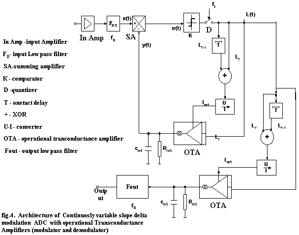
The general idea for adaptive S-D modulation is the step size adoption in the feedback path. The compandor as it is shown on fig.4 is modifying the integrator’s input in accordance of the digital structure L(t) in modulator’s output. Analysing L(t) is equal to analyse the dynamic range of the input signal. There are many companding techniques which are completely reviewed in the studied literature [10,12,13,14,16], but only 2 of them are in use nowadays: - High information adaptive Delta-Modulation and Continuously variable slope delta modulation/CVSD/.
In CVSD the step size adoption depends on two
previous values of the encoder’s output signal L(t).[3,23,24,25].-
2bit algorithm. The block
diagram for CVSD is shown on fig.2.The compandor is build by additional delay circuit/flip-flop/, thus we have the
possibilty to compare the digital values of L(t) in
rth. And (r-1)th. tact cycles. If ![]() are with values “0” or ”1” then this means that the error in
the modulator is not changing it’s polarity, then the adoption circuit
increases the integrator’s input with coefficient +A. If
are with values “0” or ”1” then this means that the error in
the modulator is not changing it’s polarity, then the adoption circuit
increases the integrator’s input with coefficient +A. If![]() are different that means the error in the modulator has been
changed and the adoption circuit decreases the integrator’s input with coefficient
–B. The XOR circuit compares the two previous values
are different that means the error in the modulator has been
changed and the adoption circuit decreases the integrator’s input with coefficient
–B. The XOR circuit compares the two previous values ![]() and controls the adoption process. Fig3. shows the
integrator’s output tracking the input.
and controls the adoption process. Fig3. shows the
integrator’s output tracking the input.

A
new practical implementation of a first order continuously variable slope
sigma-delta ADC with operational transconductance amplifiers in the feedback
path is shown on fig.4. It consists from the following main blocks: input amplifier, input low
pass filter (antialiasing filter), summer, comparator, quantizer, one tact
delay, XOR, U-I converter and operational
transconductance amplifier. The signal from the input amplifier is fed to
the antialiasing filter and removes from the input signal frequencies higher than Ft/10, where Ft
is clock frequency of the modulator. In this CVSD ADC we use the step
size adoption, which depends on two previous values of the encoder’s output, signal L(t). - 2bit
algorithm.
The
operational transconductance amplifier (OTA) together with the U-I converter and Rint, Cint represent
circuit of voltage-controlled integrator. The XOR circuit is aanalysing L(t)
that is equal to analyse the dynamic range of the input signal. If ![]() and
and ![]()
![]() in two
previous clocks are
with same values then this means that the error in the modulator is not
changing it’s polarity and the output of XOR will be “1”. This “1” will be
converted in current
in two
previous clocks are
with same values then this means that the error in the modulator is not
changing it’s polarity and the output of XOR will be “1”. This “1” will be
converted in current ![]() . The increase of
. The increase of ![]() will increase the
voltage over Rint, Cint which is equal of increasing the
step
will increase the
voltage over Rint, Cint which is equal of increasing the
step ![]() of y(t) and decreasing the value if the error signal
e(t).
of y(t) and decreasing the value if the error signal
e(t).
If ![]()
![]() и
и ![]() are different for example
are different for example ![]() =1 ,
=1 , ![]() =0, thus means
that the error signal changes during the two previous clocks and the output of XOR
will be “0”, which will be converted by U-I into
=0, thus means
that the error signal changes during the two previous clocks and the output of XOR
will be “0”, which will be converted by U-I into ![]() , where
, where ![]() . This will decrease the step
. This will decrease the step ![]() of y(t). By doing this, the integrator output will track the
input and the adoption process will extend the SNR of the ADC.
of y(t). By doing this, the integrator output will track the
input and the adoption process will extend the SNR of the ADC.
The designed from us CSVD ADC with operational transconductance
amplifiers was practical tested with operational transconductance amplifier
CA3060, and Ft=100KHz. The measurements the of ADC showed SNR
of 88db in frequency range up to 10KHz. The oversampling ratio is 10 (Ft/Fb). The ADC has a wide range of
applications such as: telecommunications, sensor interfaces, audio applications
and many others. Because of the investigations of this architecture are still
in progress, we will announce in some
our future article all the criteria used in design and simulation of this new
implementation.
References:
[1] J.Candy and G.Temes,
“Oversampling methods for A/D and D/A conversion” in Oversampling Delta-Sigma Data Converters. Pp.1-25,
IEEE pres, 1992.
[2] P.M. Asia, H.V. Sorensen and
J.Van Der Spiegel, “An overview of sigma-delta converters”, IEEE Signal
Processing Magazine, Vol.13, No.1, Jan.1996
[3]
[4] Habibi, A. “Comprasion of
Nth-Order DPCM Encoder with linear transformation and block quantization
techniques”, IEEE Transactions on Communications, December 1971, pp948-956
[5] F.Maloberti, “Non conventional
signal processing by the use of sigma delta technique: a tutorial introduction”
in Proc IEEE Int. Symp. Circ. And Syst.,
[6] V.F.Dias “Signal processing in
the sigma-delta domain” Microelectronics Journal,26,
543(1995)
[7] Analog Devices, “Sigma-Delta
conversion technology”, DSPatch –Digital Signal Processing Applications
Newsletter, winter,1990
[8] Dan Harres, “Delta-sigma
analog-to-analog converter solves tough design problems” EDN
[9] Hejn,K.,
N.P. Murphy and I.Kale, “Measurements and enhancements of multistage
sigma-delta modulators” Proc. IEE IMTC/92 Conference pp.545-551